42 74ls08 pin diagram
74LS90 Pin Configuration. The pinout diagram of the 7490-decade counter is shown here. Pin 1 is a clock pulse input of MOD 5 in IC. It’s an active LOW pin to change the state of 3 bits on output. At every high to HIGH to LOW pulse outputs on three bits will be affected. Pin 2 is used as a reset pin in the IC. 7408 Datasheet – Quad 2-Input AND Gates. This is one of the TTL IC types. Part Number : 7408, 74LS08. Function : QUAD 2-INPUT AND GATE / Low Power Schottky. This device contains four independent gates each of which performs the logic AND function. Alternate Military/Aerospace device (5408) is available. Contact a Fairchild Semiconductor Sales.
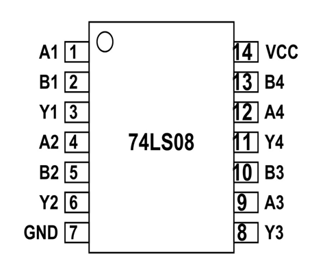
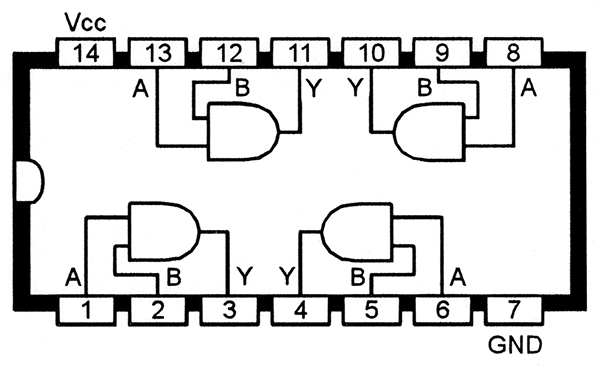
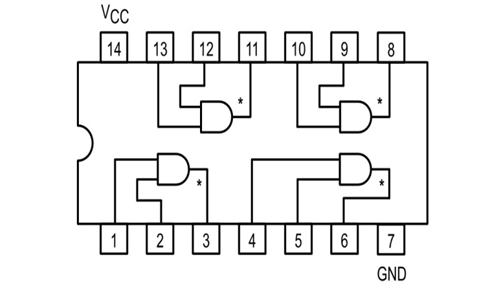
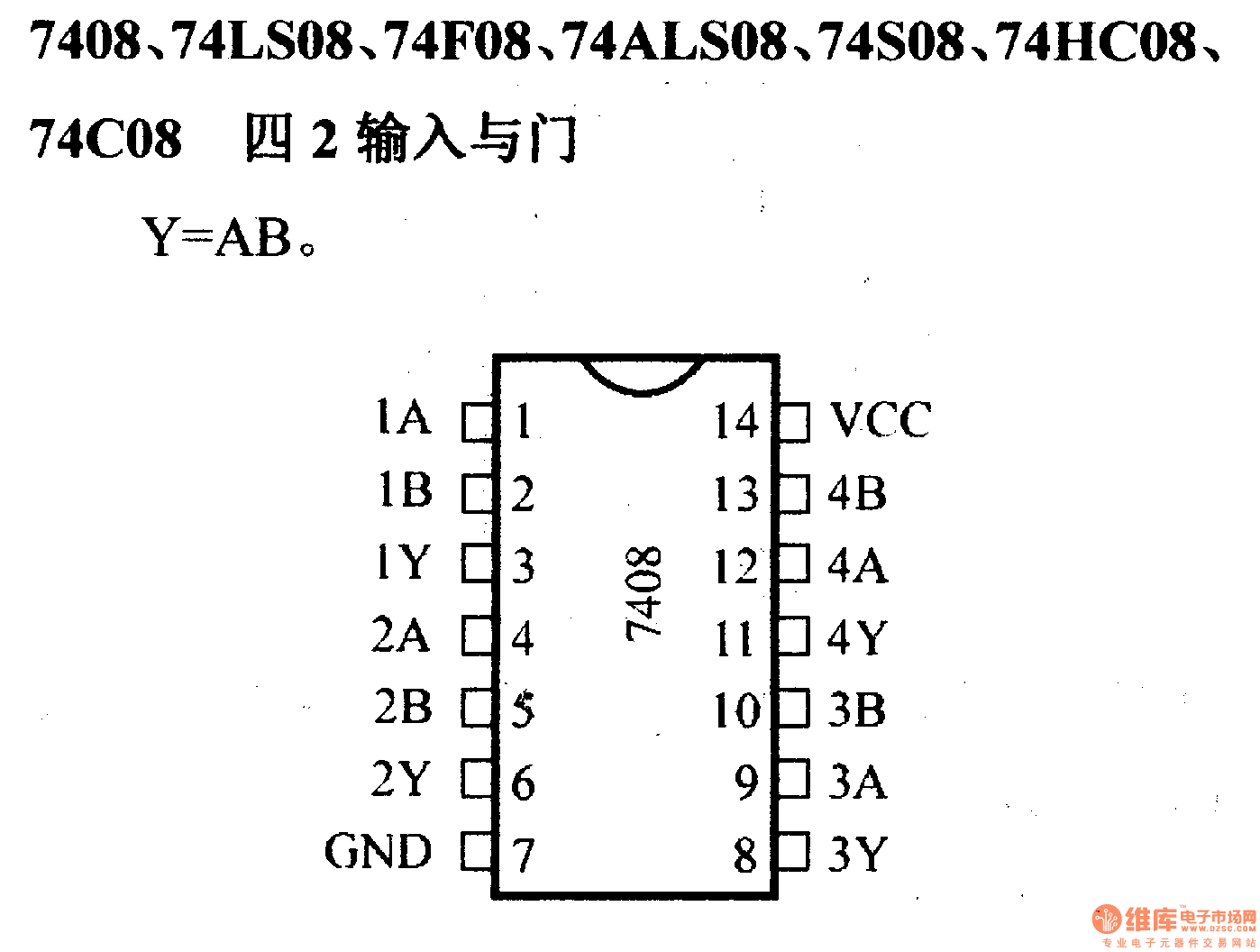
Pin Number. Description. INPUT OF INVERTING GATES. 1. 1A-INPUT of GATE 1. 3. 2A-INPUT of GATE 2. 5. 3A-INPUT of GATE 3. 9. 4A-INPUT of GATE 4. 11. 5A-INPUT of GATE 5. 13. 6A-INPUT of GATE 6. SHARED TERMINALS. 7. GND- Should be connected to ground. 14. VCC-Should be connected to positive voltage. OUTPUT OF INVERTING GATES. 2. 1Y-OUTPUT of GATE 1 ...

74ls08 pin diagram
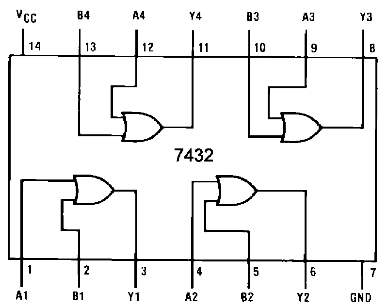
The 74LS73 is a dual in-line JK flip flop IC. It contains two independent J-K flip-flops with individual J-K, clock and direct clear inputs. The 74LS73 is a positive pulse triggered flip-flop. Available in 14-pin SOIC package . Note: Complete Technical Details can be found at the datasheet give at the end of this page. Equivalent for 74LS32: CD4071. Other Logic Gates: 74LS00, 74LS08, 74LS02, 74LS04, 74HCT04 . How to use 74LS32. 74LS32 or 74LS32N has 12 input output pins for a total of four OR gates. Pin 7 is the ground pin that provides power to the chip. Pin 14 is the Vcc terminal of the chip, and it is used to provide the chip with a power supply. Have a look at the IC 7408 pinout diagram above. IC 7408 Equivalents and Replacement Details. Equivalents of IC 7408 are IC 74LS08, HEF4081, and SN54LS08.
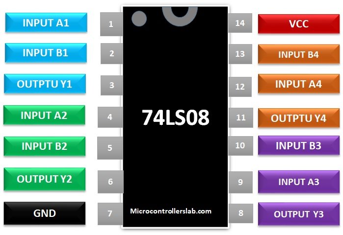
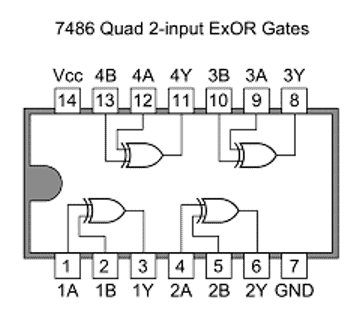
74ls08 pin diagram. The 74LS86 comes up with four XOR gates and Pin 1 will be used as the first input pin. It will use to input the data to first XOR gate within the IC. B2. Pin 2. Pin 2 will use as the second input pin. It will also use to input the data to the first XOR gate. Y1. Pin 3. Pin 3 is an output pin of the first XOR gate. 74LS73 datasheet, 74LS73 PDF, 74LS73 Pinout, Equivalent, Replacement - Dual J-K Flip-Flops(with Clear) - Hitachi Semiconductor, Schematic, Circuit, Manual Buy 74LS08 TI/MOTOROLA , Learn more about 74LS08 Quad 2-Input AND Gates, View the manufacturer, and stock, and datasheet pdf for the 74LS08 at Jotrin Electronics. 74LS08 IC is a member of 74XXYY IC series. There are four AND gates in the chip and each gate have two inputs, hence the name QUADRUPLE 2- INPUT AND GATE. The gates in the chip are designed by SCHOTTKY TRANSISTORS for high speed logic operations. 74LS08 Pin configuration. 74LS08 is a 14 PIN IC.
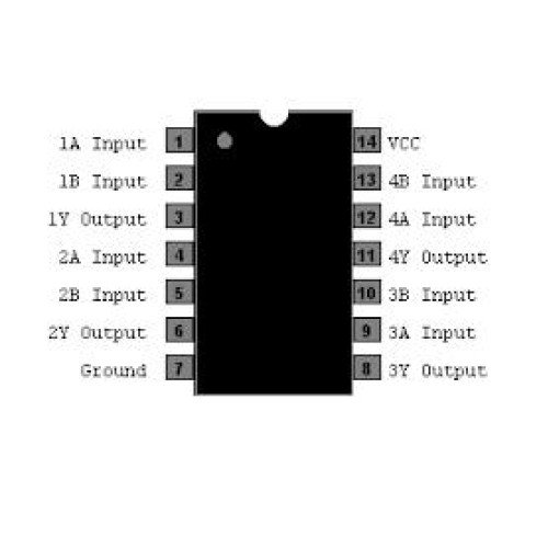
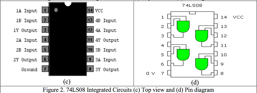
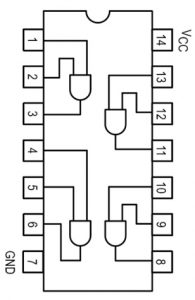
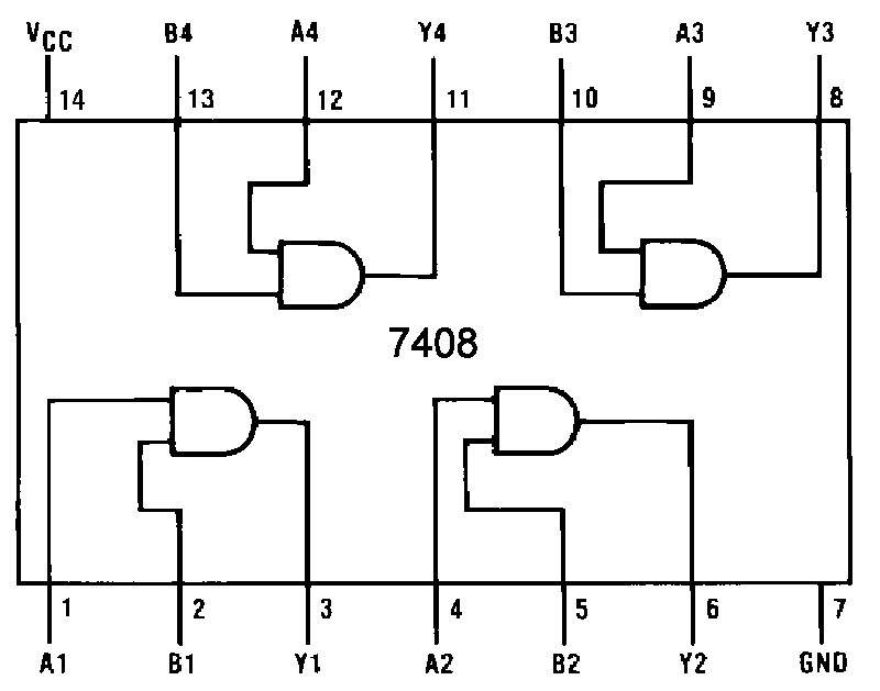
HD74LS08P DILP-14 pin PRDP0014AB-B (DP-14AV) P — HD74LS08FPEL SOP-14 pin (JEITA) PRSP0014DF-B (FP-14DAV) FP EL (2,000 pcs/reel) HD74LS08RPEL SOP-14 pin (JEDEC) PRSP0014DE-A (FP-14DNV) RP EL (2,500 pcs/reel) Note: Please consult the sales office for the above package availability. Pin Arrangement (Top view) VCC 4B 4A 4Y 3A 3B 1A GND 1B 1Y 2A ... 74LS08 is a Quadruple 8-bit Two Input AND IC. This post mainly covers the datasheet, pinout, use, voltage, and other details about the 74LS08 gate IC. Furthermore, there is a huge range of semiconductors, capacitors, resistors, and ICs in stock. Welcome your RFQ! Shown in figure below is the pin diagram of the 74LS86 Quad 2-input XOR gate. The internal structure of IC 7408 described here. 74LS08 is a 14 PIN IC. In simple terms logic gates are the electronic circuits in a digital system. The AND Gate performs the logical multiplication operation which is commonly known as AND function. 74LS08 Pin configuration ... 74LS08 is a 14 PIN IC. The chip is available in different packages and is chosen depending on requirement. The description for each ...
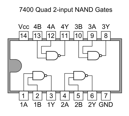
74LS00 Pin Configuration. 74LS00 is a 14 PIN device. The chip is available in different packages and is chosen depending on requirement. The description for each pin is given below. Pin Number. Description. NAND GATE 1. 1. A1-INPUT1 of GATE 1. 2. B1-INPUT2 of GATE 1. 3. Y1-OUTPUT of GATE1. NAND GATE 2. 4. Account Suspended · This Account has been suspended · Contact your hosting provider for more information 74LS08 datasheet, 74LS08 PDF, 74LS08 Pinout, Equivalent, Replacement - Quad 2-Input AND Gates - Fairchild Semiconductor, Schematic, Circuit, Manual. April 26, 2020 - 74LS73 DUAL JK FLIP-FLOP introduction, pinout, pin configuration , working, applications, features and example in proteus with steps

Electric Bugle: IC Diagrams
Nov 17, 2019 - 74LS73 DUAL JK FLIP-FLOP introduction, pinout, pin configuration , working, applications, features and example in proteus with steps

Where and How to Use SN74LS08N IC
74LS04 Pin Digram. This a pinout diagram of hex NOT gate 74LS04IC.. Other logical gates: 74LS138, 74LS00, 74LS02 74LS04 IC PIN CONFIGURATION Details This table lists 74ls04 NOT gate details of all pins.

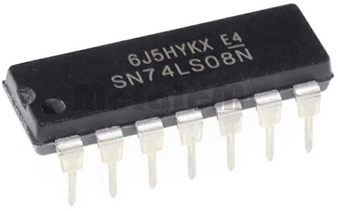
Electrical Equipment & Supplies 2 pieces SN74LS08N Quad 2 ...
November 25, 2019 - First, take the IC 74LS08 in proteus the attach it to the logic gates. The apply each and every logic. First, apply both inputs LOW. You may notice that OUTPUT is LOW which is according to the truth table. ... The apply one logic HIGH and other one LOW. First Apply first input pin HIGH, you ...
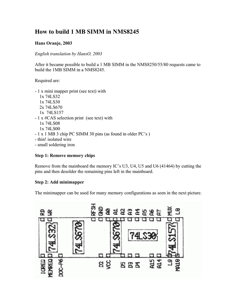
How to build 1 MB SIMM in NMS8245 | Manualzz
23. sep. 2021 ... SN74LS08N Pinout. 74LS08 Pin configuration. Features. Product Attributes. 74LS08 Equivalents. Where to Use 74LS08 IC ? How to Use 74LS08 IC ...

In a certain manufacturing process, a conveyor belt will shut ...
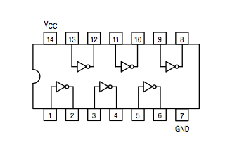
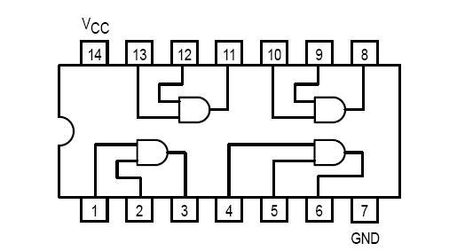
September 23, 2021 - The 74LS08 is one of the most affordable AND logic ICs on the market. It is extremely popular and widely available. ... TTL outputs are provided by the chip, which are required in some systems. ... The four AND gates in the chip mentioned earlier are connected internally as shown in diagram below.

74ls Series Logic IC, Sn74ls11n DIP-14 Logic Gates Triple 3 ...
74LS73, 74LS73 Datasheet, 74LS73 Dual JK Flip-Flop Datasheet, buy 74LS73
How Logic Gates Work - Homemade Circuit Projects
74LS08 pin configuration. Abstract: 74LS08 function table. Text: GD54/ 74LS08 QUADRUPLE 2-INPUT POSITIVE AND GATES Description Pin Configuration This device ...
DeldSim - 8 Bit Comparator Using 74LS85
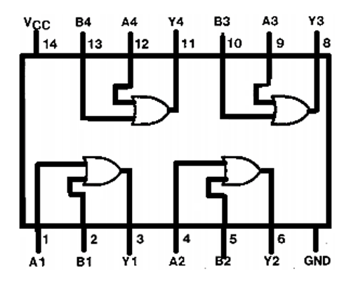
pin 14 = vcc pin 7 = gnd logic diagram 2 b1 6 y2 4 a2 5 b2 8 y3 9 a3 10 b3 11 y4 12 a4 13 b4 y = ab pinout: 14 ...
Binary to GRAY Code Converter, Design of a Two to Four ...
CONNECTION DIAGRAM DIP (TOP VIEW) NOTE: The Flatpak version has the same pinouts (Connection Diagram) as the Dual In-Line Package. PIN NAMES LOADING (Note a) HIGH LOW A1-A4 Operand A Inputs 1.0 U.L. 0.5 U.L. ... LOGIC DIAGRAM C0 A1 B1 A2 B2 A3 B3 A4 B4 VCC = PIN 16 ...

Pin on 74LS Series Datasheet
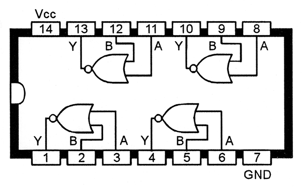
Specify by appending the suffix letter “X” to the ordering code. Connection Diagram. Function Table. Y = AB. H = HIGH Logic Level. L = ...

IC7408, 74HC08, 74ls08 Logical AND gate experiment with full video explanation - DLD 1
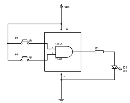
Use the datasheet to confirm the pin diagram of the IC, its function table, and operating conditions such as typical value of VCC and its absolute maximum ratings. Ensure that your operating conditions are within the limits given in the datasheets. 3. Place the 74LS08 IC on the breadboard. 4. Connect +5V to pin #14, and GND to pin #7 of the IC. 5.
CD4071 OR Gate IC Datasheet : Working & Its Applications
Pin 5 will be used to give the second input to the second AND gate in IC 74LS08. Y2: Pin 6: Pin 6 will be used to receive the output of second AND gate from IC. GND: Pin 7: Pin 7 is a ground pin; it will be used as common ground by other communication devices with IC and Power Supply. Y3: Pin 8

How to Use 74LS32, 74LS08 and 74LS04 ICs in Multisim
74LS02 Quadruple 2-Input NOR Gate IC. 74LS IC series comes up with multiple gates. It provides us with compact design and multiple packages of the same IC. Here we will discuss 74LS02. 74LS02 also know as 7402. IT comes up with 4 internal NOR gate. IC 7402 comes up in multiple packages with 14 pins and 2 inputs 4-NOR gates. NOR gate is designed ...
74LS08 Pinout, Configuration, Equivalents, Circuit & Datasheet
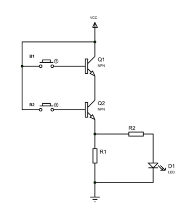
The J and K pins are the input pins for the Flip-Flop and the Q and Q bar pins are the output pins. Input pins are pulled down to ground through a 1k resistor, this way we can avoid the pin in floating condition. That is the pin will held to ground when the button is not pressed and when the button is pressed the pin will be held to supply voltage.
Robomart Product Catalog
The page you are looking for might have been removed, had its name changed, or is temporarily unavailable · Please check the address bar to make sure the link is typed correctly, use the links below to locate the information you want, or search the site for another destination

74LS08 AND Gate IC Pinout Examples Features Datasheet ...
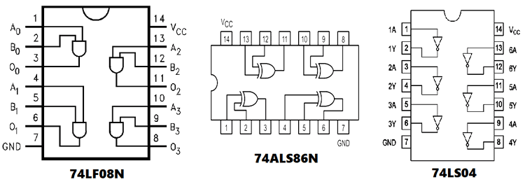
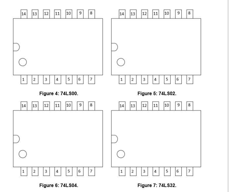
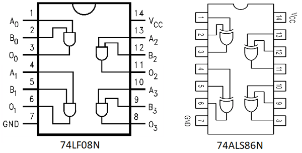
1. Find the datasheet of the 74LS08 Integrated circuit board online and complete the following pinout diagrams: (Save a copy of the datasheet for future reference) a. Write down the pin numbers in the smaller boxes. b. Sketch the internal circuit of the Integrated Circuit (IC) 74LS08 in Figure 3. C.
74LS08 Pinout, Configuration, Equivalents, Circuit & Datasheet
7473 Dual JK Flip-Flop with Clear Datasheet, SN7473, buy ic 7473
74LS08 Quad 2-Input AND Gate Buy Online in India - Robomart
January 14, 2021 - 74LS08 Quadruple IC is a member of the 74XXYY IC series. In this article, we will take a look into the key features & specs of 74LS08 2-Input AND gate IC.
CSC231 Logic Design Lab 2014 - dftwiki3
Jameco Electronics carries thousands of electronic components including power, semiconductors and test equipment. Paypal accepted.

IC 7408 Pin Diagram, Circuit Design, Data Sheet, Application ...
Pin#13 is an input pin and used to feed carry in. Pin#15,2,6,9 are output pins and will be used to observe the addition of two above numbers as S4 S3 S2 S1. Pin# 14 is an output pin and displays the resultant carry of addition. Internal Logic Diagram. The logic diagram implemented inside 74LS83 using gates is given below for more clarity.
Understanding Digital Buffer, Gate, and Logic IC Circuits ...
Pin 2: Pin 2 represents the second bit of 4-bit input data of the IC. LT' Pin 3: Pin 3 is known as the lamp test pin. It is used to make all the output pins HIGH to test all the 7-segment led. It's an active low pin. BI'/BRO' Pin 4: Pin 4 will act as a reset pin. In case of LOW state on pin 4, there won't be any output.
Solved TTL Digital Logic Design Problem (2) 74LS08 IC A ...
IC 7408 is a logic gate IC. It consists of four two-input AND Gates. The IC 7408 has total fourteen pins including ground and Vcc. The simple pin diagram is shown here. The internal structure of IC 7408 described here. Pin Description of IC 7408 explained in detail. Application of IC 7408 given here.
74LS08 Pinout, Configuration, Equivalents, Circuit & Datasheet
The pin 3 should be provided with a clock source normally a PWM signal from an MCU or 555 timers is used. The pin can be used to clear the data and reset the flip flop by making it high. The complete working of the Flip flop can be understood by taking at the function table below. The symbol "X" indicates don't care and the up-arrow ...
PPT - LOGIC DESIGN AND CIRCUITS PowerPoint Presentation, free ...
Pin 7 is the ground pin that provides power to the chip. Pin 14 is the Vcc terminal of the chip, and it is used to provide the chip with a power supply. Have a look at the IC 7408 pinout diagram above. IC 7408 Equivalents and Replacement Details. Equivalents of IC 7408 are IC 74LS08, HEF4081, and SN54LS08.
74LS08 AND Gate IC Datasheet : Working & Its Applications
Available in 14-pin SOIC package . Note: Complete Technical Details can be found at the datasheet give at the end of this page. Equivalent for 74LS32: CD4071. Other Logic Gates: 74LS00, 74LS08, 74LS02, 74LS04, 74HCT04 . How to use 74LS32. 74LS32 or 74LS32N has 12 input output pins for a total of four OR gates.
Digital Circuits for High School Students (Part 1)
The 74LS73 is a dual in-line JK flip flop IC. It contains two independent J-K flip-flops with individual J-K, clock and direct clear inputs. The 74LS73 is a positive pulse triggered flip-flop.
And Gate Ic Number : 74ls135 Quad 2 Input Xor Logic Gate Ic ...
Digital Circuits for High School Students (Part 1)

Digital Logic AND Gate

Computer Science - All Logic gates introduction, how gates ...
Understanding Digital Buffer, Gate, and Logic IC Circuits ...
74LS08 AND Gate IC Pinout Examples Features Datasheet ...
74LS08 AND Gate IC Datasheet : Working & Its Applications

7408 Technical Data
How Logic Gates Work - Homemade Circuit Projects
Half Subtractor Circuit and Its Construction
Solved 1. Find the datasheet of the 74LS08 Integrated | Chegg.com
Half Adder Circuit: Theory, Truth Table & Construction
74LS32 OR Gate Datasheet, Pinout, Equivalent & Specs
74 series digital circuit of 7408 74LS08 quad-2 input nand ...

74LS08 AND Gate IC Pinout Examples Features Datasheet ...
74LS08 Selling Leads, Price trend, 74LS08 DataSheet download ...


Comments
Post a Comment